Overview
The purpose of the circuit designed in this project was to display a set of 8 numbers in order, my birthday, on a common cathode display using only switches which are flipped in a binary order. To achieve the goal, I had to use boolean algebra, Karnaugh mapping, a bread board, and was allowed any type of 74SL gate chip. Resistors were also necessary for the inputs not damaging display, but they were built into my breadboard already.
Truth Table
Truth tables are used to visualize what combinations will output true, or a one. Zero represents no output, or false. This table shows what combination of outputs need to occur in order for certain segments of the display to light up and output a number.

In this table, the letters a-g along the top represent different segments of the seven segment display, and each different combination of inputs will have a digit assigned them which is created by an assortment of segments lit up due to the inputs. The X, Y, and Z are placeholders for the eventual real-world switches that will be used for inputs. Lastly, any Xs in the table are representing that it does not matter whether the segment is lit up or not, and that the last two arrangements of inputs are not used and do not affect the circuit.
Karnaugh Maps and Segment Logic Simplification

K-mapping is a way of getting the simplest form of a logic expression based on a truth table without having to manually simplify any expressions. It works by, first, labeling the sides starting with the first two inputs in pairs in an "not-not, not-normal, normal-normal, normal-not" arrangement along one of the vertical sides. The top side can be labeled by simply "not, normal" with the third input. Next you put in the outputs (1, 0, or X) in left to right, top to bottom order, except for the last two groups of two inputs which switch places on the table. Finally, to get your simplified logic expression, you group any ones by circling either 2, 4, or 8 at a time with no 0s in between, and the more 1s circled at a time the more simplified the expression is. Circles do not need to obey boundaries and can link, for example, two from the very top, to two on the very bottom. Also, circles can include Xs, but they do not need to be circled otherwise.
K-mapping is better than Boolean algebra in this instance because of how many inputs and outputs there are. You would not have to risk making a mistake while simplifying with Boolean algebra and its many steps, but K-mapping is visual and has fewer steps. All expressions are shown in sum-of-products form, and the reason there are seven logic expressions is because there are seven segments that need to light up under different conditions, though three of the seven expressions repeat and do not need to be constructed twice.
K-mapping is better than Boolean algebra in this instance because of how many inputs and outputs there are. You would not have to risk making a mistake while simplifying with Boolean algebra and its many steps, but K-mapping is visual and has fewer steps. All expressions are shown in sum-of-products form, and the reason there are seven logic expressions is because there are seven segments that need to light up under different conditions, though three of the seven expressions repeat and do not need to be constructed twice.
Multisim Implementation
Blow is the digitally simulated circuit using the Multisim software that contains the logic expressions in gate form that I found using the K-maps. There are grounds, switches, resistors, a 7-segment display, digital sources, a bus, and nand gates used.

This circuit is in bus form and uses nine 74SL00 NAND gates, which would in theory require three NAND gate chips and four 200ohm resistors. There are instances in the circuit above where NAND inverters could have been saved if I had tapped the outputs of other NAND inverters and used them for other expressions, allowing me to make a two chip, seven gate circuit. The purpose of the resistors are to not give too much power to the segments of the display or else risk overloading and breaking it.
I am using a common cathode seven segment display, but there is also a type called a common anode display. Common cathode diplays are grounded and require an input to light up its segments, while common anode displays are powered and only light up in the absence of an input. Both have seven possible inputs with each individual one, labeled A to G, light up different segments in a clockwise order, starting from the top segment and ending at the middle.
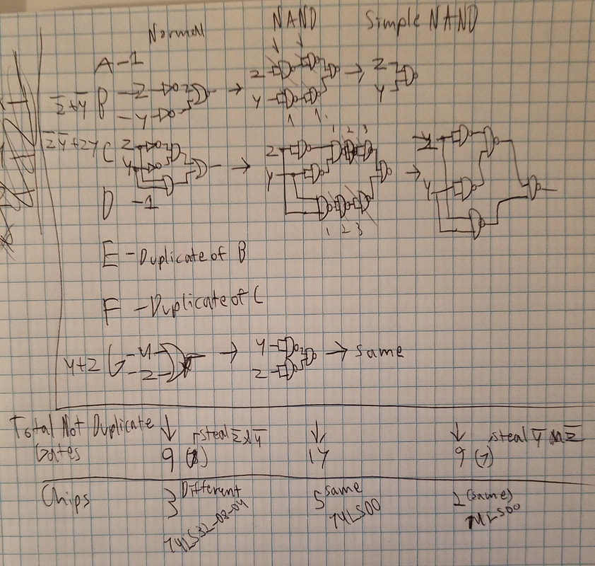
While I could have made the circuit out of inverters, AND, and OR gates, I chose to use all NAND because I knew that it would lessen the difficulty of wiring since it might require less gates and certainly decrease the number of chips over all since NAND (and NOR) gates have the special properties to construct all three of the normal gates with only their type. Once I had a converted every inverter, AND, and OR gate, I canceled out any repeating instances of a NAND inverter since leaving it would waste gates. In the end I was left with a circuit that would require two of the same chip as opposed to three different (And, OR, invert) chips.
Below is my work: (Extra Credit)
I am using a common cathode seven segment display, but there is also a type called a common anode display. Common cathode diplays are grounded and require an input to light up its segments, while common anode displays are powered and only light up in the absence of an input. Both have seven possible inputs with each individual one, labeled A to G, light up different segments in a clockwise order, starting from the top segment and ending at the middle.
While I could have made the circuit out of inverters, AND, and OR gates, I chose to use all NAND because I knew that it would lessen the difficulty of wiring since it might require less gates and certainly decrease the number of chips over all since NAND (and NOR) gates have the special properties to construct all three of the normal gates with only their type. Once I had a converted every inverter, AND, and OR gate, I canceled out any repeating instances of a NAND inverter since leaving it would waste gates. In the end I was left with a circuit that would require two of the same chip as opposed to three different (And, OR, invert) chips.
Below is my work: (Extra Credit)
Bill of Materials

This table shows how many of each material was used. As a side note, the breadboard had the display, switches, and resistors all integrated, and wires are not accounted for.
Bread-Boarding
With this being my second bread boarding experience, I felt that it was much easier than before for a couple reasons. First, I double checked every wire which ultimately led to there being only one malfunctioning segment on the first try which was later fixed. Next, I decided to use all NAND chips since I felt would not only use less chips since it would use only one gate the whole time, but I also knew I would find it easier to keep track of only one type instead of multiple different types. Lastly, I felt that I had more knowledge of common mistakes in general. In the end, the only troubleshooting I did (with the aid of the teacher) was switching the place of one wire in order to make the g (middle) segment of the display function as it should. i would say that a great skill I've learned is to convert circuits to use only one type of gate and chip when at all possible since I found that it makes the job easier.
Conclusion
As previously stated, I learned that it is useful to convert circuits to use one type of gate when possible, but aside from that, I learned how seven segment displays can receive different inputs to output a desired symbol or digit. Next time, since I felt that I did every other aspect of the project to the best of my ability, I would simply manage my time better and not wait so long to do the website especially. I fully understood the entire project and have no further questions about any of the concepts. K-mapping is useful because it provides an easier way to derive a simplified logic expression from a truth table, avoiding the need to use Boolean algebra which could otherwise lead to mistakes.
I enjoyed this project a lot and had fun wiring while feeling confident in my ability to construct a circuit using simplified logic expressions derived from K-mapping and truth tables, as well as my ability to convert a AOI circuit into a NAND/NOR only circuit.
I enjoyed this project a lot and had fun wiring while feeling confident in my ability to construct a circuit using simplified logic expressions derived from K-mapping and truth tables, as well as my ability to convert a AOI circuit into a NAND/NOR only circuit.
