Overview
My task was to design a counter similar to one in a deli which counts up from 0, stops and stays at 80, and can be cleared to reset. We were required to use certain parts for this project such as seven segment displays, 74LS93 gates, and D Flip-Flop gates.
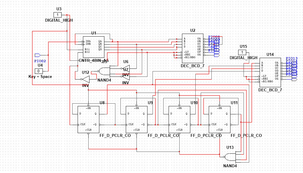
Multisim Circuit

|
PLD Circuit
|
Some differences between default mode and PLD mode are that there are much less options for components in general, pins, and naming schemes. First, in any of the categories of components, there are much less choices. Sources, for example, has only five different options, while the default mode easily has over one or two hundred. Pins are a component only in PLD mode, and they serve as simulated place holders for the real-world pins on whatever device you are uploading it to, and you can use both input pins and output pins. These combined with the upload ability allow you to transfer your circuit into the real world, something you can not do within the default mode. Uploading is fairly simple with the Multisim software, you simply need the external device connected to the computer, then select Transfer> Export to PLD, and then wait for it to either succeed or fail to upload, both of which it will tell you at the bottom of the screen in the results tab. The main use of the default mode of Multisim is to plan out a circuit you will later build in real life with specific components, and PLD is a simpler method of making a test circuit but is not actually practical for use making a circuit outside of a PLD device aside from getting the basic idea of what you are making.
Bill of Materials
In this project I used the following items:
A powered breadboard, lots of wire, the PLD upload device, and two seven segment displays.
This short list is an example of how much easier it is to work with the PLD device.
A powered breadboard, lots of wire, the PLD upload device, and two seven segment displays.
This short list is an example of how much easier it is to work with the PLD device.
Conclusion
Questions:
Difference between SSI and MSI circuits?
SSI circuit utilize basic gates and small chips in low numbers while MSI circuits use complicated chips with hundreds of transistors in them in circuits, such as the 74LS74/93 chips in my circuits above.
Limitations of my MSI circuit?
The only limitation I could think of in my circuit was that the ones place of the two-digit deli counter has to start at zero due to the chip that was used. 93's don't allow any other starting number.
What is the Ripple Effect?
It is a term used when talking about asynchronous counters made with Flip-Flop gates, and is defined by the odd flickering that occurs whenever an output changes. Each gate in the counter has to wait for the previous gate to change, and this causes a minor delay in each following gate's output which is really only seen if it is slowed down. The output indicator will flicker with different values before stopping at the desired number after a fraction of a second.
Explain the process your circuit goes through when running.
First, I press a switch or the automatic clock changes output and this travels into the clock input of the 74LS93 gate. The signal is interpreted by the gate and increases the binary output by one, which is then taken in by the demultiplexer and converted into a seven-segment display output that is one digit greater than the last. While the output of the 93 is being converted, a NAND gate is checking when the output reaches a binary ten, and will reset the 93 counter upon detecting it, yet since this detection happens so quickly, it would not be visible to the human eye that a ten, or an A on the display, was displayed, making it a 0-9 counter. Then, once a 10 is reached by the 93 counter, a signal is sent down to the 0-8 counter below it that is made of 74s. The signal tells the first 74 to switch output when it goes into the clock input, and then the first 74 outputs a signal every second time it receives an input. This repeats for all four of these 74s, and each change in output by each chip is sent to both a NAND and a demultiplexter. The demultiplexer converts the positive Q outputs of these chips into a seven-segment interpretation output, and a seven segment display outputs the current state of all the 74s. The NAND is set to detect a binary 9 output from the 74s so that it will then reset the counter back to zero. Also, the method of resetting the counters with the NANDs goes as follows: Then NAND detects a number and outputs a low value, and this is sent to either the four clear inputs on the 74s, or the R02 input on the 93.
I did not have the time to add a hold value function or a reset all function.
Did my classmates have any differences in their solutions?
Unfortunately I did not have the time to ask anyone about their solutions.
